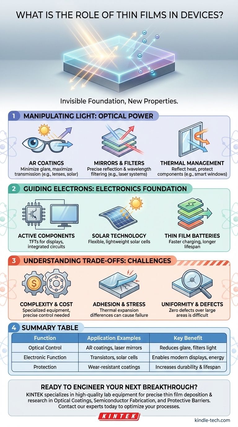
가장 근본적인 수준에서 박막의 역할은 표면에 미세한 재료 층을 적용하여 해당 표면에 그렇지 않으면 가질 수 없는 완전히 새로운 속성을 부여하는 것입니다. 이러한 엔지니어링된 층은 현대 기술의 보이지 않는 기반이며, 안경의 반사 방지 코팅부터 스마트폰 내부의 복잡한 회로, 태양 전지의 효율성에 이르기까지 모든 것을 가능하게 합니다.
박막의 핵심 기능은 단순히 표면을 코팅하는 것이 아니라, 해당 표면이 빛, 전기, 열 또는 물리적 환경과 상호 작용하는 방식을 정밀하게 설계하는 것입니다. 원자 규모에서의 이러한 제어가 수많은 현대 장치의 성능과 기능을 가능하게 하는 요소입니다.
빛 조작: 박막의 광학적 힘
박막 기술의 상당 부분은 빛의 흐름을 제어하는 데 전념하고 있습니다. 특정 재료를 하나 이상 증착함으로써 우리는 어떤 파장이 반사, 투과 또는 흡수되는지를 정확하게 결정할 수 있습니다.
투과율 및 효율성 향상
반사 방지(AR) 코팅은 주요 예시입니다. 이는 카메라 렌즈와 안경부터 태양 전지 및 전자 디스플레이에 이르기까지 모든 곳에 사용됩니다.
이러한 코팅은 자연적인 반사를 줄이도록 정밀하게 설계된 층으로, 눈부심을 최소화하고 표면을 통과하는 빛의 양을 최대화합니다. 이는 태양 전지의 효율성이나 디스플레이의 선명도를 직접적으로 향상시킵니다.
반사 제어 및 필터링
박막은 매우 특수한 거울과 필터를 만드는 데 필수적입니다. 예를 들어, 고출력 레이저 시스템은 분산 브래그 반사기(교대로 쌓인 박막 스택)를 사용하여 특정 파장에 대해 거의 100% 반사되는 거울을 만듭니다.
마찬가지로, 다른 재료를 층으로 쌓아 엔지니어들은 매우 좁은 대역의 빛을 차단하는 노치 필터나 가시광선은 통과시키면서 적외선 열은 반사하는 건축용 유리 코팅을 만들 수 있습니다.
열 에너지 관리
박막은 열 관리에 있어서도 중요한 역할을 합니다. 필라멘트 램프 내부에는 열을 필라멘트로 다시 반사하여 밝기와 효율성을 높이는 적외선 반사 코팅이 증착됩니다.
데이터 저장 장치나 창문에서는 특정 박막이 열 장벽 역할을 하여 민감한 부품을 온도 급변으로부터 보호하거나 건물 내부로 열이 들어오는 것을 방지합니다.
전자 흐름 유도: 현대 전자공학의 기반
전체 반도체 산업은 박막의 정밀한 증착을 기반으로 구축됩니다. 집적 회로 내부의 미세한 트랜지스터와 경로는 전도성, 절연성, 반도성 박막을 층으로 쌓아 구성됩니다.
능동 부품 구축
박막 트랜지스터(TFT)는 LCD 및 OLED 화면을 포함한 현대 평판 디스플레이의 중추입니다. 디스플레이의 각 픽셀은 증착된 박막으로 만들어진 자체의 작은 트랜지스터에 의해 제어됩니다.
이러한 동일한 원리는 유연성, 경량화 및 향상된 에너지 효율성과 같은 이점을 제공하는 박막 태양 전지 및 배터리 제작을 가능하게 합니다.
신에너지 기술 구현
박막 기술은 재생 에너지 및 저장 분야의 발전을 주도하고 있습니다. 박막 태양 전지는 유연한 기판 위에 생산될 수 있어 기존 실리콘 패널이 비실용적인 새로운 응용 분야를 열어줍니다.
마찬가지로, 박막 배터리는 더 빠른 충전 속도와 더 긴 수명을 약속하며, 이는 가전제품부터 전기차에 이르기까지 모든 것에 중요합니다.
상충 관계 이해
박막 기술은 엄청나게 강력하지만, 구현에는 어려움이 따릅니다. 이러한 층을 증착하는 과정은 재료 과학의 고도로 전문화된 분야입니다.
복잡성과 비용
박막 증착은 종종 진공 챔버와 같은 정교한 장비와 층 두께를 제어하기 위한 극도의 정밀도(때로는 원자 한 층까지)를 요구합니다. 이로 인해 제조 공정이 복잡하고 잠재적으로 비용이 많이 들 수 있습니다.
재료 접착 및 응력
일반적인 실패 지점은 박막과 그것이 적용된 기판 사이의 접착입니다. 열팽창 또는 내부 응력의 차이로 인해 필름이 갈라지거나 벗겨지거나 박리되어 장치가 쓸모없어질 수 있습니다.
균일성과 결함
넓은 영역에 걸쳐 결함이 없는 완벽하게 균일한 필름을 얻는 것은 극도로 어렵습니다. 보호 코팅의 단 하나의 미세한 핀홀이나 불순물이라도 전체 장벽을 손상시킬 수 있으며, 광학 코팅의 불균일성은 그 성능을 망칠 수 있습니다.
목표에 맞는 올바른 선택
올바른 박막 전략은 엔지니어링하려는 기능적 속성에 전적으로 달려 있습니다.
- 광학 성능에 중점을 둔 경우: 유전체 또는 금속 필름의 적층 구조를 활용하여 특정 광 파장의 반사, 투과 및 흡수를 정밀하게 제어합니다.
- 전자 기능에 중점을 둔 경우: 반도체, 도체 및 절연체 필름을 증착하고 패터닝하는 데 집중하여 트랜지스터나 에너지 장치와 같은 능동 부품을 구축합니다.
- 기계적 또는 화학적 보호에 중점을 둔 경우: 마모, 부식 및 기타 환경 요인에 대한 내구성 있는 장벽을 만들기 위해 특정 세라믹 또는 금속과 같은 단단하고 불활성인 재료를 우선시합니다.
박막이 재료 속성을 근본적으로 엔지니어링하는 도구라는 점을 이해하면 거의 모든 기술 분야에서 새로운 성능과 가능성을 열 수 있습니다.
요약표:
| 기능 | 응용 예시 | 주요 이점 |
|---|---|---|
| 광학 제어 | 반사 방지 코팅, 레이저 거울, 열 차단 창 | 눈부심 감소, 빛 필터링, 열 관리 |
| 전자 기능 | 트랜지스터(TFT), 집적 회로, 태양 전지 | 현대 디스플레이, 컴퓨팅 및 에너지 생성을 가능하게 함 |
| 기계적/화학적 보호 | 내마모성 코팅, 부식 방지 장벽 | 부품의 내구성과 수명 향상 |
박막으로 다음 혁신을 엔지니어링할 준비가 되셨나요?
박막은 고급 광학 장치, 차세대 전자 장치 또는 효율적인 에너지 솔루션을 개발하든 관계없이 장치의 우수한 성능을 잠금 해제하는 열쇠입니다. KINTEK은 정밀한 박막 증착 및 연구에 필요한 고품질 실험 장비와 소모품을 제공하는 데 전문성을 가지고 있습니다.
당사의 전문 지식은 다음 분야에서 귀하의 혁신을 지원합니다.
- 광학 코팅: 빛의 투과 및 반사에 대한 정밀한 제어 달성.
- 반도체 제조: 균일한 층으로 안정적인 전자 부품 구축.
- 보호 장벽: 견고하고 접착력 있는 필름으로 제품 내구성 강화.
KINTEK이 재료 과학 분야의 파트너가 되도록 하십시오. 오늘 전문가에게 문의하여 당사의 솔루션이 박막 공정을 최적화하고 가장 진보된 아이디어를 실현하는 데 어떻게 도움이 될 수 있는지 논의하십시오.
시각적 가이드
관련 제품
- 박막 증착용 알루미늄 코팅 세라믹 증착 도가니
- 박막 증착용 텅스텐 증착 보트
- 전자빔 증착 코팅 무산소 구리 도가니 및 증착 보트
- 고온 응용 분야를 위한 몰리브덴 텅스텐 탄탈 증발 도가니
- 리튬 배터리 포장용 알루미늄-플라스틱 연성 포장 필름


