"범위"에 대해 이야기할 때, 우리는 단일 측정 기준을 말하는 것이 아니라 네 가지 주요 차원에 걸친 이 기술의 광범위한 범위를 의미합니다. 물리적 두께는 일반적으로 수 나노미터에서 수 마이크로미터에 이릅니다. 더 중요하게도, 그 범위는 엄청나게 다양한 재료, 광범위한 기능적 특성, 그리고 마이크로칩부터 의료 기기에 이르기까지 끊임없이 확장되는 첨단 기술 응용 분야 목록을 포함합니다.
박막 기술의 핵심 개념은 단순히 물리적 치수가 아니라 다목적 플랫폼으로서의 기능입니다. 나노스케일에서 재료 층을 정밀하게 제어함으로써, 벌크 재료에서는 달성할 수 없는 고유한 광학적, 전기적, 기계적 특성을 엔지니어링할 수 있습니다.
정의하는 "범위": 필름 두께
가장 문자 그대로의 "범위" 해석은 두께입니다. 이 차원은 모든 다른 특성이 발생하는 기반입니다.
단일 원자에서 마이크로미터까지
박막은 원자 한 층(나노미터의 일부)에서 수 마이크로미터(µm)까지 두께가 달라질 수 있는 재료 층입니다.
대부분의 산업 응용 분야는 10나노미터에서 10마이크로미터 범위 내에서 작동합니다. 이 규모는 재료가 고유한 특성을 나타낼 만큼 얇으면서도 견고하고 기능적일 만큼 충분히 두꺼운 최적의 지점입니다.
두께가 중요한 이유
이러한 작은 치수에서는 벌크 재료에서는 무시할 수 있는 효과가 지배적이 됩니다. 여기에는 양자 역학적 현상, 광학 간섭, 고유한 응력-변형률 관계가 포함되며, 엔지니어는 두께를 조정하는 것만으로 재료의 성능을 미세 조정할 수 있습니다.
재료 및 공정의 범위
박막 기술의 다재다능함은 증착될 수 있는 광범위한 재료와 이를 수행하는 방법의 정밀도와 직접적으로 연결됩니다.
금속에서 첨단 세라믹까지
사실상 모든 종류의 재료를 박막으로 만들 수 있습니다. 참고 자료에는 광범위한 선택 항목이 포함되어 있습니다.
- 금속: 알루미늄, 내화 금속
- 유전체 및 세라믹: 산화규소, 질화물(TiN)
- 반도체: 실리콘, 게르마늄, 화합물 반도체(GaAs)
- 특수 재료: 다이아몬드 유사 탄소(DLC), 그리고 신흥 비정질 산화물
이러한 재료의 다양성은 거의 모든 엔지니어링 과제에 맞게 조정된 코팅을 만드는 것을 가능하게 합니다.
정밀도를 가능하게 하는 공정
이러한 필름을 생성하려면 고도로 제어된 환경과 정교한 장비가 필요합니다. 주요 방법은 다음과 같습니다.
- 화학 기상 증착(CVD): 전구체 가스를 사용하여 표면에 필름을 "성장"시키며, 균일하고 고순도인 층을 만드는 데 이상적입니다.
- 물리 기상 증착(PVD): 진공 상태에서 고체 재료를 기화(스퍼터링 또는 증발)시킨 후 기판에 응축시키는 방식으로, 금속 및 경질 코팅에 탁월합니다.
- 이온 주입: 전하를 띤 원자(이온)를 표면에 주입하여 화학적 및 물리적 특성을 변경합니다.
달성 가능한 특성의 스펙트럼
재료를 박막으로 증착하는 것은 벌크 재료와 다른 특정 기능적 특성을 얻기 위해 수행됩니다.
광학 특성 조작
박막은 빛을 제어하는 데 매우 중요합니다. 디스플레이를 위해 고도로 투명하게, 렌즈를 위해 반사 방지되게, 또는 거울을 위해 고도로 반사되게 엔지니어링될 수 있습니다.
전기적 거동 제어
필름의 전기적 특성은 정밀하게 조정될 수 있습니다. 마이크로칩 배선에서 전도체로, 커패시터에서 절연체(유전체)로, 또는 트랜지스터에서 반도체로 작용할 수 있습니다.
기계적 내구성 향상
박막은 종종 보호 코팅으로 사용됩니다. 질화티타늄(TiN) 및 다이아몬드 유사 탄소(DLC)와 같은 재료는 절삭 공구 및 마모 부품을 위한 초경질, 긁힘 방지 및 저마찰 표면을 만듭니다.
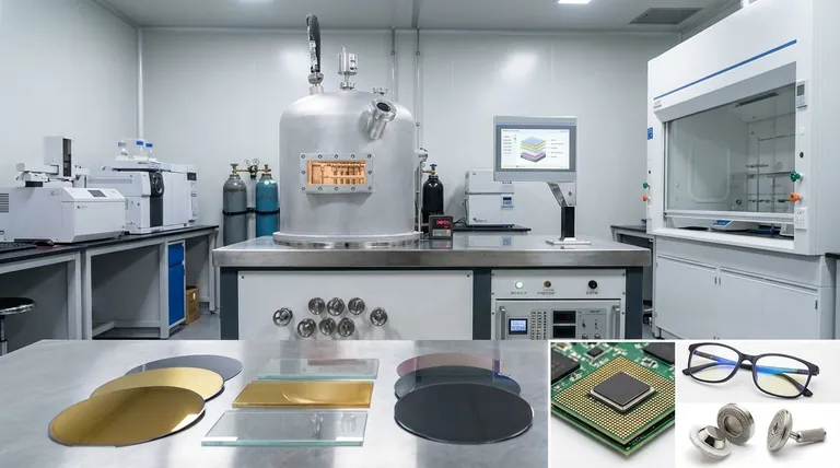
현대 응용 분야의 폭넓은 범위
재료와 특성의 조합은 박막에 현대 기술을 정의하는 매우 광범위한 응용 분야를 제공합니다.
- 반도체 제조: 모든 집적 회로의 기초를 형성하며, 실리콘 웨이퍼 위에 트랜지스터, 배선 및 절연체를 만듭니다.
- 디스플레이 및 광학: 평판 TV 및 스마트폰 화면부터 코팅된 안경 및 고성능 렌즈에 이르기까지 모든 것을 가능하게 합니다.
- 데이터 저장: 하드 드라이브의 자기층과 광학 디스크의 상변화층을 만드는 데 사용됩니다.
- 의료 기기: 임플란트를 위한 생체 적합성 코팅과 수술 도구를 위한 내구성 있고 멸균된 표면을 제공합니다.
내재된 트레이드오프 이해하기
박막 기술은 강력하지만 도전과 한계가 없는 것은 아닙니다. 이러한 점을 이해하는 것이 성공적인 응용에 중요합니다.
비용 및 복잡성
CVD 및 PVD와 같은 증착 공정을 위한 장비는 비싸며 작동 및 유지보수를 위해 상당한 전문 지식이 필요합니다. 이는 제조에 대한 높은 진입 장벽을 만듭니다.
기판 의존성
박막은 기판(실리콘 웨이퍼 또는 유리 조각 등) 위에 증착되어야 합니다. 필름의 접착력, 응력 및 최종 특성은 이 기판의 선택 및 표면 처리에 매우 의존적입니다.
내구성과 안정성
극도로 얇은 층은 부서지기 쉽고 긁힘, 박리 또는 환경적 열화에 취약할 수 있습니다. 원하는 특성(예: 투명도)을 달성하는 것은 종종 장기적인 내구성과 상충될 수 있습니다.
목표에 따라 '범위'를 구성하는 방법
박막 기술의 "범위"는 특정 목표의 렌즈를 통해 가장 잘 이해됩니다.
- 재료 과학 또는 R&D에 중점을 둔 경우: 비정질 산화물과 같은 새로운 재료 조합의 범위는 혁신에 가장 중요한 영역입니다.
- 제조 및 엔지니어링에 중점을 둔 경우: 증착 공정(CVD, PVD)의 범위와 일관된 필름 특성을 달성하기 위해 이를 제어하는 능력은 주요 변수입니다.
- 제품 개발에 중점을 둔 경우: 광학에서 전자공학 등에 이르는 응용 분야의 범위는 이 기술이 경쟁 우위를 제공할 수 있는 시장 기회를 정의합니다.
궁극적으로 박막은 미세 규모에서 물질을 엔지니어링할 수 있는 힘을 제공하는 기반 기술입니다.
요약표:
| 범위의 측면 | 주요 세부 사항 |
|---|---|
| 두께 | 단일 원자(<1 nm)에서 수 마이크로미터(µm)까지 |
| 재료 | 금속(Al, Ti), 세라믹(TiN), 반도체(Si, GaAs), DLC |
| 주요 특성 | 광학(투명도), 전기(전도성), 기계(경도) |
| 주요 응용 분야 | 반도체, 디스플레이, 데이터 저장, 의료 기기 |
정밀 박막으로 우수한 표면을 엔지니어링할 준비가 되셨습니까? KINTEK은 박막 증착(CVD, PVD) 및 분석을 위한 첨단 실험실 장비 및 소모품을 전문으로 합니다. R&D 또는 제조 분야에 관계없이 당사의 솔루션은 일관되고 고성능의 코팅을 달성하는 데 도움이 됩니다. 귀하의 특정 실험실 요구 사항을 논의하고 혁신을 가속화하는 방법에 대해 논의하려면 지금 전문가에게 문의하십시오.
시각적 가이드

관련 제품
- 박막 증착용 알루미늄 코팅 세라믹 증착 도가니
- 박막 증착용 텅스텐 증착 보트
- 전자빔 증착 코팅 무산소 구리 도가니 및 증착 보트
- 고온 응용 분야를 위한 몰리브덴 텅스텐 탄탈 증발 도가니
- 리튬 배터리 포장용 알루미늄-플라스틱 연성 포장 필름


