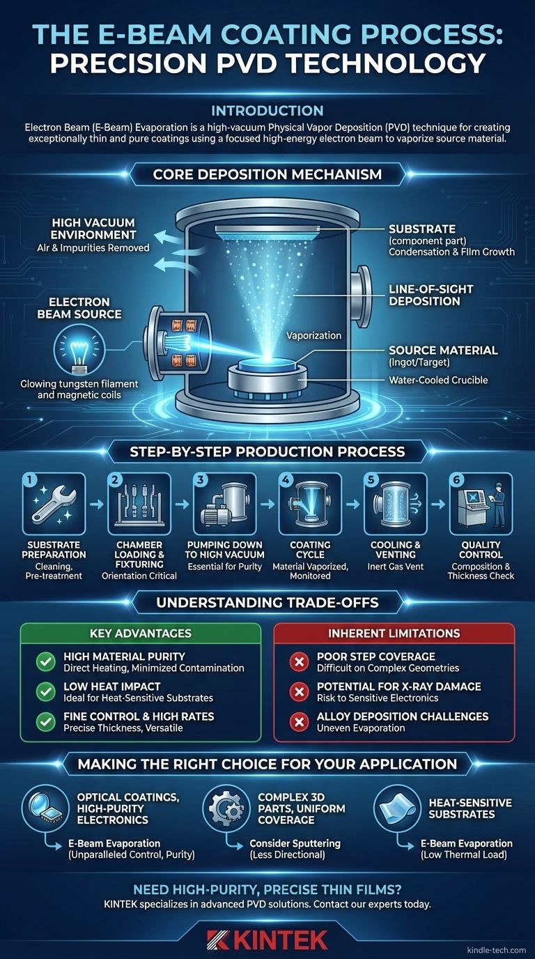
전자빔(E-Beam) 증착은 매우 얇고 순수한 코팅을 생성하는 데 사용되는 고진공 물리 기상 증착(PVD) 기술입니다. 이 공정은 집중된 고에너지 전자빔을 사용하여 소스 재료를 가열하여 기화시킵니다. 이 증기는 직선으로 이동하여 기판에 응축되어 정밀한 원자 단위의 막을 형성합니다.
전자빔 코팅은 기본적으로 정밀도와 코팅되는 부품에 대한 낮은 열 영향으로 높이 평가되는 시선 증착 공정입니다. 특수 응용 분야를 위한 극도로 순수하고 밀도가 높은 필름을 생성하는 데 탁월하지만, 그 방향성으로 인해 복잡한 3차원 형상을 코팅하는 데 어려움이 있습니다.
핵심 증착 메커니즘
전자빔 공정을 이해하려면 진공 챔버 내에서 발생하는 핵심 물리학을 파악하는 것이 중요합니다. 각 단계는 특정 필름 구성 및 두께를 달성하기 위해 정밀하게 제어됩니다.
진공 환경
전체 공정은 고진공 챔버 내에서 이루어집니다. 챔버를 비우는 것은 증발된 재료와 반응하여 최종 필름을 오염시킬 수 있는 공기 및 기타 기체 불순물을 제거하는 데 중요합니다. 이 거의 진공 상태는 또한 증기 원자가 다른 입자와 충돌하지 않고 기판으로 직접 이동할 수 있도록 합니다.
전자빔 소스
텅스텐 필라멘트가 가열되어 전자 흐름을 생성합니다. 이 전자들은 음극선관(CRT) 텔레비전과 유사하게 일련의 자기장을 사용하여 가속 및 집중되어 고에너지 빔을 형성합니다.
소스 재료 기화
이 집중된 전자빔은 수냉식 구리 도가니에 담긴 소스 재료(종종 잉곳 또는 타겟이라고 함)에 직접 조사됩니다. 빔의 강렬한 에너지는 재료를 끓는점까지 가열하여 증발 또는 승화시켜 증기를 생성합니다.
시선 증착
증기 원자는 소스에서 기판으로 직선으로 직접 이동합니다. 이 "시선" 특성은 코팅이 증발 소스에서 직접 보이는 표면에만 증착됨을 의미합니다.
응축 및 필름 성장
증기 원자가 상대적으로 차가운 기판 표면에 도달하면 응축됩니다. 이 과정은 코팅 층을 원자 단위로 쌓아 올려 매우 미세하고 밀도가 높은 박막을 만듭니다.
단계별 생산 공정
핵심 메커니즘에서 산업 응용 분야로 이동하려면 일련의 신중하게 관리되는 생산 단계가 필요합니다.
1단계: 기판 준비
깨끗한 표면 없이는 적절한 접착이 불가능합니다. 이 단계에는 오염 물질을 제거하기 위한 엄격한 세척이 포함됩니다. 부품의 이력에 따라 오래된 코팅을 벗겨내거나 표면을 준비하기 위한 특정 전처리도 포함될 수 있습니다.
2단계: 챔버 로딩 및 고정
소스 재료는 도가니에 놓이고 기판은 특수 고정 장치 또는 홀더에 장착됩니다. 이러한 고정 장치의 방향은 공정의 시선 특성으로 인해 중요하며, 대상 표면이 증기 흐름에 올바르게 노출되도록 합니다.
3단계: 고진공으로 펌핑
로딩 후 챔버는 밀봉되고 목표 압력 수준으로 진공화됩니다. 이 펌프 다운은 상당한 시간이 걸릴 수 있지만 최종 코팅의 순도를 위해 필수적입니다.
4단계: 코팅 주기
진공이 설정되면 전자빔이 활성화되고 재료가 기화됩니다. 증착 속도와 최종 두께는 실시간으로 모니터링되어 필름이 정밀한 사양을 충족하는지 확인합니다. 전체 주기는 재료 및 원하는 두께에 따라 30분에서 몇 시간까지 다양할 수 있습니다.
5단계: 냉각 및 환기
목표 두께에 도달하면 전자빔이 비활성화됩니다. 시스템은 냉각된 후 챔버는 불활성 가스로 환기되어 대기압으로 돌아갑니다.
6단계: 품질 관리
각 배치는 엄격한 검사를 거칩니다. 기술자는 X선 형광(XRF) 기계와 같은 도구를 사용하여 코팅의 구성과 두께를 확인하고 모든 필수 표준을 충족하는지 확인합니다.
장단점 이해
어떤 단일 코팅 기술도 모든 응용 분야에 완벽하지 않습니다. 전자빔 증착은 이상적인 사용 사례를 정의하는 뚜렷한 장점과 한계를 가지고 있습니다.
주요 장점
- 높은 재료 순도: 전자빔은 전체 도가니가 아닌 소스 재료만 직접 가열하여 오염을 최소화하고 탁월하게 순수한 필름을 만듭니다.
- 낮은 열 영향: 이 공정은 다른 방법에 비해 기판으로 전달되는 열이 적기 때문에 플라스틱, 폴리머 또는 사전 조립된 전자 부품과 같은 열에 민감한 재료를 코팅하는 데 이상적입니다.
- 정밀 제어 및 높은 속도: 증착 속도와 필름 두께를 매우 정밀하게 제어할 수 있으며, 금속 및 세라믹을 포함한 광범위한 재료에 대해 매우 높은 증발 속도를 달성할 수 있습니다.
내재된 한계
- 불량한 스텝 커버리지: 고도로 방향성 있는 증기 흐름은 복잡한 모양, 날카로운 모서리 또는 내부 표면을 균일하게 코팅하기 어렵게 만듭니다. 주로 "볼 수 있는" 부분만 코팅합니다.
- X선 손상 가능성: 고에너지 전자가 소스 재료와 상호 작용하면 X선이 생성될 수 있습니다. 일반적으로 낮은 수준이지만, 이는 매우 민감한 전자 기판 또는 광학 부품을 손상시키기에 충분할 수 있습니다.
- 합금 증착의 어려움: 증기압이 다른 여러 원소(합금)로 만들어진 재료는 휘발성이 더 높은 원소가 먼저 증발하기 때문에 증발시키기 어려울 수 있습니다.
응용 분야에 적합한 선택
올바른 PVD 방법을 선택하려면 공정 기능을 주요 엔지니어링 목표와 일치시켜야 합니다.
- 주요 초점이 광학 코팅 또는 고순도 전자 제품인 경우: 전자빔 증착은 필름 두께, 순도 및 밀도에 대한 탁월한 제어를 제공하며, 이는 이러한 응용 분야에 중요합니다.
- 주요 초점이 균일한 커버리지로 복잡한 3D 부품을 코팅하는 경우: 모든 표면이 적절하게 코팅되도록 스퍼터링과 같이 방향성이 덜한 PVD 방법을 고려해야 합니다.
- 주요 초점이 열에 민감한 기판을 코팅하는 경우: 전자빔 공정의 낮은 열 부하는 폴리머 또는 섬세한 사전 조립 부품과 같은 재료를 보호하는 데 탁월한 선택입니다.
궁극적으로 전자빔 증착을 선택하는 것은 최종 필름 품질과 정밀도가 균일한 기하학적 커버리지보다 더 중요한 응용 분야에 대한 전략적 결정입니다.
요약표:
| 주요 측면 | 세부 정보 |
|---|---|
| 공정 유형 | 물리 기상 증착(PVD) |
| 환경 | 고진공 |
| 메커니즘 | 시선 증착 |
| 주요 장점 | 고순도, 낮은 열 영향, 정밀한 두께 제어 |
| 이상적인 용도 | 광학 코팅, 고순도 전자 제품, 열에 민감한 기판 |
| 한계 | 복잡한 3D 형상에 대한 불량한 커버리지 |
연구 또는 생산을 위해 고순도 정밀 박막이 필요하십니까?
KINTEK은 까다로운 응용 분야를 위한 PVD 솔루션을 포함한 고급 실험실 장비를 전문으로 합니다. 당사의 전문 지식은 특정 기판 및 목표에 대한 우수한 필름 품질, 순도 및 성능을 보장하기 위해 올바른 코팅 기술을 선택하는 데 도움이 될 수 있습니다.
오늘 전문가에게 문의하여 귀하의 실험실 박막 증착 요구 사항을 지원하는 방법을 논의하십시오.
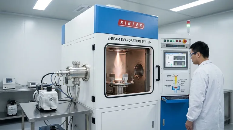
시각적 가이드
관련 제품
- 고온 응용 분야를 위한 전자빔 증착 코팅 텅스텐 도가니 및 몰리브덴 도가니
- 전자빔 증착 코팅 전도성 질화붕소 도가니 BN 도가니
- 증착용 전자빔 증착 코팅 금도금 텅스텐 몰리브덴 도가니
- 전자빔 증착 코팅 무산소 구리 도가니 및 증착 보트
- 전자빔 증착용 고순도 순수 흑연 도가니


