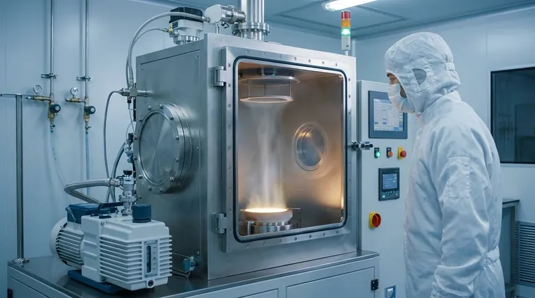
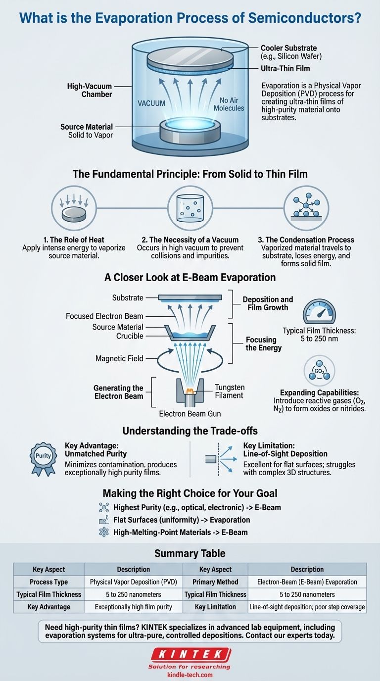
반도체 분야에서 증착(Evaporation)은 실리콘 웨이퍼와 같은 기판 위에 재료의 초박막을 형성하는 데 사용되는 물리적 기상 증착(PVD) 공정입니다. 이 공정은 고진공 챔버 내에서 소스 재료를 가열하여 기체로 변환하는 과정을 포함합니다. 이 기체 상태의 원자들은 진공을 통해 이동하여 더 차가운 기판 위에 응축되어 고체 상태의 고순도 박막을 형성합니다.
증착의 핵심 원리는 진공 상태에서 열에너지를 사용하여 고체 재료를 증기로 변환한 다음, 이 증기가 목표 표면에 정밀하게 제어되는 얇은 층으로 재고체화되는 것입니다. 이 방법은 마이크로프로세서와 집적 회로에서 발견되는 복잡한 구조를 구축하는 데 필수적입니다.
기본 원리: 고체에서 박막까지
증착의 본질은 원자 수준의 구성을 위해 설계된 3단계 공정입니다. 각 단계는 최종 박막의 품질과 무결성을 보장하는 데 중요합니다.
열의 역할
이 공정은 작은 펠릿이나 잉곳 형태의 소스 재료에 강렬한 에너지를 가하는 것으로 시작됩니다. 목표는 재료의 온도를 증발점까지 높여 증발(또는 승화, 고체에서 기체로 직접 이동)하게 만드는 것입니다.
진공의 필요성
이 전체 공정은 고진공 환경 내에서 이루어집니다. 진공은 증발된 원자와 충돌하여 궤도를 벗어나게 하거나 박막에 불순물을 유입시킬 수 있는 공기 및 기타 기체 분자를 제거하기 때문에 매우 중요합니다.
응축 공정
방해받지 않는 경로를 통해 증발된 재료는 소스 위에 전략적으로 배치된 기판으로 직접 이동합니다. 차가운 기판 표면에 접촉하면 원자는 열에너지를 잃고 응축되어 표면에 결합하면서 원하는 박막을 점차적으로 형성합니다.
전자빔 증착(E-Beam Evaporation)의 자세한 이해
여러 가열 방법이 있지만, 전자빔(e-beam) 증착은 정밀도와 광범위한 재료 처리 능력 덕분에 반도체 산업에서 지배적인 기술입니다.
전자빔 생성
이 공정은 고온으로 가열되어 전자의 흐름을 방출하는 텅스텐 필라멘트에서 시작됩니다. 이 전자들은 고전압 필드에 의해 가속됩니다.
에너지 집중
강력한 자기장이 이 고에너지 전자들을 안내하고 십자형 빔으로 집중시키는 데 사용됩니다. 이 빔은 도가니(crucible)라고 불리는 용기에 담긴 소스 재료에 정밀하게 지향됩니다.
증착 및 박막 성장
전자빔의 강렬한 에너지는 소스 재료를 녹인 다음 증발시킵니다. 생성된 증기는 위로 흐르면서 기판 위에 증착되어 매우 높은 순도의 박막을 만듭니다. 최종 코팅 두께는 엄격하게 제어되며, 일반적으로 5~250나노미터 범위입니다.
반응성 가스를 이용한 기능 확장
E-빔 공정은 화합물을 생성하도록 조정될 수 있습니다. 증착 중에 챔버 내에 산소나 질소와 같은 반응성 가스를 주입하면 웨이퍼 위에 금속 산화물이나 질화물과 같은 비금속 박막을 형성할 수 있습니다.
트레이드오프 이해하기
증착은 강력한 기술이지만, 모든 엔지니어링 공정과 마찬가지로 특정 응용 분야에 적합성을 결정하는 특정 장점과 한계가 있습니다.
주요 장점: 탁월한 순도
E-빔 증착의 주요 이점은 매우 높은 순도의 박막을 생성할 수 있다는 것입니다. 전자빔에 의해 소스 재료만 직접 가열되므로 가열 장치나 도가니로 인한 오염이 최소화됩니다.
주요 한계: 시선(Line-of-Sight) 증착
증착은 방향성이 있는 시선 공정입니다. 원자는 소스에서 기판으로 직선으로 이동합니다. 따라서 평평한 표면 코팅에는 탁월하지만, 언더컷이나 트렌치가 있는 복잡한 3차원 구조를 균일하게 코팅하는 데는 어려움이 있습니다.
목표를 위한 올바른 선택
올바른 증착 방법을 선택하는 것은 박막과 제조되는 장치의 특정 요구 사항에 전적으로 달려 있습니다.
- 가장 높은 박막 순도 달성이 주요 관심사라면: 특히 민감한 광학 또는 전자층의 경우 E-빔 증착이 종종 우수한 선택입니다.
- 비교적 평평한 표면에 박막을 증착하는 경우: 증착은 단순한 형상에 대해 우수한 균일성과 제어를 제공합니다.
- 고융점 금속 또는 특정 유전체를 증착해야 하는 경우: 전자빔의 집중된 에너지는 이러한 견고한 재료를 효과적으로 증발시킬 수 있는 몇 안 되는 방법 중 하나입니다.
증착은 현대 마이크로일렉트로닉스의 복잡한 세계를 구축하는 데 필요한 정밀한 적층을 가능하게 하는 기초 기술입니다.
요약표:
| 주요 측면 | 설명 |
|---|---|
| 공정 유형 | 물리적 기상 증착(PVD) |
| 주요 방법 | 전자빔(E-Beam) 증착 |
| 일반적인 박막 두께 | 5~250 나노미터 |
| 주요 장점 | 극도로 높은 박막 순도 |
| 주요 한계 | 시선 증착; 낮은 스텝 커버리지 |
반도체 R&D 또는 생산을 위한 고순도 박막이 필요하신가요?
KINTEK은 반도체 제조의 정밀한 요구 사항을 충족하기 위해 증착 시스템을 포함한 첨단 실험실 장비를 전문으로 합니다. 당사의 솔루션은 차세대 마이크로프로세서 및 집적 회로 구축에 중요한 초순수 제어 증착을 달성하는 데 도움이 됩니다.
지금 바로 전문가에게 문의하여 당사의 증착 기술이 연구소의 역량을 어떻게 향상시킬 수 있는지 논의해 보세요.
시각적 가이드
관련 제품
- 증착용 전자빔 증착 코팅 금도금 텅스텐 몰리브덴 도가니
- 고온 응용 분야를 위한 전자빔 증착 코팅 텅스텐 도가니 및 몰리브덴 도가니
- 전자빔 증착 코팅 무산소 구리 도가니 및 증착 보트
- 반구형 바닥 텅스텐 몰리브덴 증착 보트
- 전자빔 증착용 고순도 순수 흑연 도가니


